
ITL's processes and capabilities have developed from our original mission to optimize imaging sensors for backside illumination in order to improve their quantum efficiency and spectral response range. Those processing requirements have developed into capabilities which can now be applied to a wide variety of semiconductor devices, some of which we describe below.
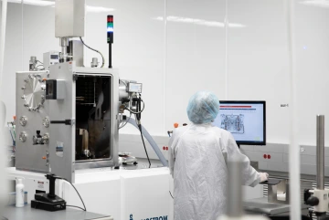
PROBE TESTING
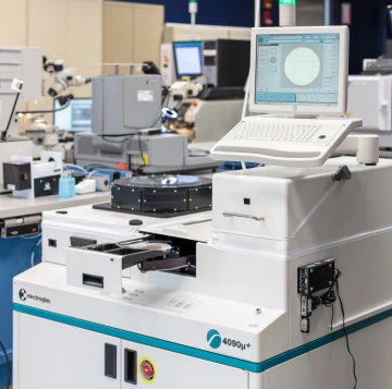
Wafer Prober - Electroglas EG 4090u
We characterize hybridized semiconductor die as well as entire wafer lot runs before proceeding with other processing steps. Our tests include DC measurements for shorts and opens, AC functionality, and imaging tests for defects, charge transfer efficiency, noise, and gain. These are the same performance characteristics evaluated in the final step of a fully packaged sensor. We can perform these tests at temperatures as low as -60C.
ITL, with original funding from the National Science Foundation, developed cold CCD wafer probing systems to quantitatively characterize sensors at the wafer and die level. The goals of these systems has been to evaluate devices before proceeding with subsequent laboratory processing steps as well as to provide rapid feedback to manufacturers concerning device performance, particularly for new devices and technologies.
WAFER DICING
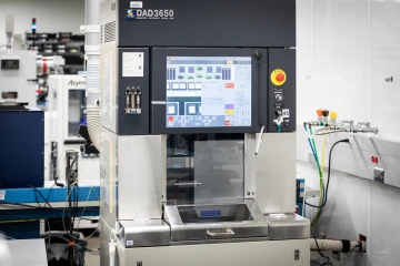
Dicing Saw - Disco DAD 3650
Our wafer dicing saw is needed to cut (or dice) the individual devices from the round wafers on which they are fabricated. We also dice the hybridization bonding substrates which are used in some fabrication steps.
Our saw has automation capabilities and can be used to dice a number of materials, including silicon, glass, and ceramics. It includes a high-conductance water-feed system which reduces static charge build-up during dicing which can lead to Electrostatic Discharge (ESD) failure of the sensitive devices. A unique feature of our DISCO DAD3650 saw is that it has been custom fitted with an IR camera which allows dicing silicon wafers and die from the backside.
HYBRIDIZING – FLIP CHIP BONDING
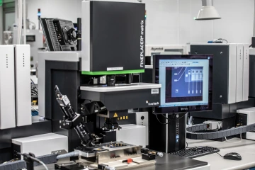
Die Bonder - Finetech FINEPLACER matrix
Our back-illuminated sensors are flip-chip bonded or hybridized to attach their front side to a stable support substrate. This process also allows electrical interconnection from the sensor's front side bonding pads to matching pads on the substrate. Bumps are placed on the bonding pads prior to flip-chip bonding.
We have both fully automated and manual stud bumping machines to apply bumps to devices. We have three different hybridizers which can be used to align the devices and substrates and then apply the necessary heat and pressure.
A important goal of our sensor optimization has been to produce a flat and stable imaging surface . The flip-chip process allows this because the sensor is forced against a custom silicon or ceramic support substrate. To ensure mechanical stability, we subsequently underfill epoxy between the device and substrate.
SILICON SENSOR ETCHING
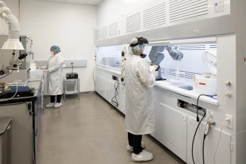
Chem lab for acid etching processes
The heart of our sensor optimization is backside etching or thinning.
We have designed and constructed a suite of linear agitation thinning machines which move the sensor in an acid bath. Uniformity to better than one micron is obtained with this method. Etching is done in an acid mixture selective to p+ silicon. Thinning is accomplished on a die basis. We use a wax border to protect the front-side device circuitry and substrate traces from being attacked by the acid. We have successfully thinned devices as large as a 10kx10k 9-micron pixel CCD.
We use a second acid etch to remove any remaining p+ silicon and to remove stains which sometimes form on the surface. This etch is non-selective and can therefore be used to thin into the epitaxial layer to tailor device thickness, if necessary. Resolution may also be improved by ultra-thinning the device to eliminate any field-free region in the CCD. We make use of this fact to ultra-thin devices to be used in applications requiring the highest possible spatial resolution.
THIN FILMS DEPOSITION AND ANALYSIS
Coating Chamber - Angstrom Engineering
One of the most significant quantum efficiency losses of back illuminated sensors is reflection off their back surface. The thinning process creates a mirror-like finish with an extremely high specular reflectivity. This reflection loss approaches 60% in the UV. The application of a thin film antireflection (AR) coating directly onto the sensor back surface can therefore significantly increase QE.
ITL has pioneered the development of high efficiency AR coatings for back illuminated sensors. We have found several suitable materials for silicon AR coatings, including hafnium oxide (HfO2), tantalum pentoxide (Ta2O5) and magnesium fluoride (MgF2).
For permanent backside charging, we apply a Chemisorption Coating (developed at ITL) to produce a net negative charge on the detector back surface. There is no backside damage using this process which would cause QE-temperature instabilities and/or reduce the maximum QE obtained.
PACKAGING AND WIRE BONDING
Wire bonder - K&S Ball Bonder 4524A
Packaging is accomplished by mounting the processed semiconductor device, such as a CCD or COS imager, to a package of some form. We typically design each substrate to fit into a specific package. Each electrical trace on the substrate leads from a bump to a wire bonding pad. Commercial packages are often not flat enough for large area devices and so we design and fabricate custom packages as well.
We utilize standard thermo-compression wire bonding to form electrical connections between the various components. To verify the reliability of our wire bonds, we can pull test each to the required MIL-STD specification.
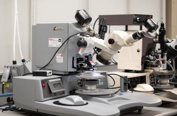
METROLOGY
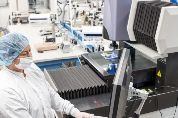
CMM - VIEW Summit 600
We often perform a detailed measurement of device surface position after fabrication. This includes flatness as well as position relative to defined package coordinate system. Typical measurement accuracy is about two microns although much finer measurements can be made in specific cases.
We have a VIEW Summit 600 Coordinate Measuring Machine (CMM), a Zygo interferometric microscope, and other profilometry equipment to perform these measurements. Our equipment is in an ESD safe, cleanroom environment.
SENSOR CHARACTERIZATION
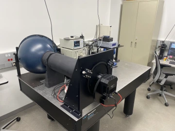
Testing and characterization bench
We have developed software and hardware systems for sensor characterization, usually aimed at fully testing CCDs for scientific applications.
We also provide detector testing as a service to the community for a nominal fee. Our goal is to provide rapid feedback of device performance using well proven and calibrated techniques. All the testing is automated and script driven, requiring no operator intervention once the device is set up. We have developed an automated system using an open-source Python library for measuring quantum efficiency (QE), read noise, gain, full well capacity, linearity, photoresponse non-uniformity, dark current, defect counts, and dark-current non-uniformity, and charge transfer efficiency (CTE).